

news +insights
Applied Materials Opens $5B EPIC Center With Four Acres of Cleanroom
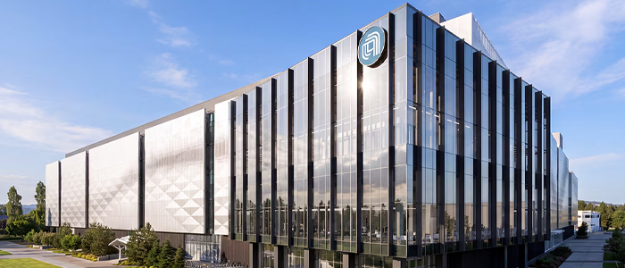
Applied Materials has opened its EPIC Center in Sunnyvale, California, a 600,000 square foot semiconductor research facility with nearly four acres of cleanroom space and a planned capital investment of about $5 billion, the company announced on October 12, as reported by ConstructConnect and Fortune.
What Happened
The Equipment and Process Innovation and Commercialization Center sits on Applied Materials' Sunnyvale campus near its headquarters Fortune. Applied describes it as the world's largest facility for collaborative research and development in semiconductor process technology and manufacturing equipment Evertiq. Fortune reported that the company calls it the largest U.S. investment ever made in advanced semiconductor equipment R&D.
The $5 billion figure is a target, not a single check. Capital spending is expected to scale up to that level over time as customer projects get underway Evertiq.
The Building
The construction numbers released with the opening show the scale of the job. The project required more than 6 million construction hours ConstructConnect. Its foundation used enough concrete to fill 34 Olympic sized pools, and the structure contains enough steel to build two Eiffel Towers. Thirty four roof trusses span the cleanrooms, each nearly 300 feet long and roughly as heavy as a dozen school buses.
Fortune described the project as a two year build and said the cleanrooms, where researchers pattern circuits onto silicon wafers, cover the area of three football fields Fortune. Evertiq gave the building as about 55,700 square meters with about 1.6 hectares of cleanroom Evertiq, consistent with the 600,000 square foot and four acre figures. None of the three outlets named the general contractor or architect.
Who Will Work There
The founding partners are TSMC, Intel, Samsung Electronics, Micron and SK hynix ConstructConnect. Innovation partners are Broadcom, Advantest, SCREEN, KIOXIA and Besi. Research partners are Arizona State University, Rensselaer Polytechnic Institute, Stanford, UC Berkeley and UCLA. Evertiq reported that more companies are expected to join over time Evertiq.
The center is for research only, not commercial chip production. Applied says co-locating its engineers with customers can cut the typical path from concept to commercialization from 10 to 12 years to as little as six Fortune. Competing chipmakers such as Micron and SK hynix will have private test facilities inside the building, each working with dedicated Applied teams. "There's never been an inflection like this in our lifetimes," CEO Gary Dickerson told Fortune.
TSMC Chairman and CEO C.C. Wei said in the announcement that working with Applied beyond the 2 nanometer node gives TSMC "early access to the disruptive equipment technologies that define the future" Evertiq.
Context
The opening comes as Applied's business is growing. Fortune reported August quarter revenue of $9.12 billion, up 25 percent from a year earlier Fortune. Several EPIC partners are also building production capacity in the United States, including Micron in Central New York and SK hynix in Indiana, both covered on this site.
Implications for Owners, Developers, Contractors and Subs
- R&D facilities now rival fabs in complexity. Four acres of cleanroom, 300 foot trusses and 6 million work hours put this research building in the same class as many production plants. Owners planning advanced labs should expect fab level MEP, vibration and contamination control requirements.
- Long span structure is a schedule driver. Column free cleanroom bays depend on heavy trusses, crane planning and steel fabrication lead times. Steel and erection subs with that experience will stay in demand.
- Specialty trades remain the bottleneck. Cleanroom ceilings, process piping, high purity gas and exhaust systems and controls require certified crews. Subs who can staff those scopes have pricing leverage across the semiconductor build out.
- Capital follows in phases. Applied's spending ramps with customer projects, so tenant fit outs and tool installs inside the shell could keep specialty contractors busy for years after opening.
- Equipment innovation feeds plant design. Faster commercialization of new tools may change utility loads and layouts in future fabs, so design teams on New York and Midwest projects should watch what comes out of Sunnyvale.
What to Watch
- Additional partners joining the center and the pace of the spending ramp toward $5 billion.
- Whether Applied names its construction and design team or releases further project details.
- Follow on investment by partners in U.S. fabs that adopt tools developed at EPIC.
Bottom Line
The EPIC Center is a large, finished example of how the chip industry is spending on U.S. construction beyond the fabs themselves. For contractors, it confirms steady demand for cleanroom, process and heavy structural work tied to semiconductors, the same demand visible in projects such as GlobalFoundries' Malta expansion and SK hynix's Indiana packaging fab.
Related Coverage
- GlobalFoundries to Add Malta Fab Capacity Under $2 Billion TSMC Interposer Deal
- SK hynix Breaks Ground on $4B Indiana AI Memory Packaging Fab
- National Grid Plans Eight 345kV Lines and 2-Mile Gas Pipeline for Micron's Clay Fabs
- $500B in U.S. Factories Under Construction as $3.4T Pipeline Waits
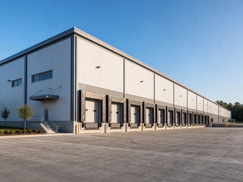
Image credit: Applied Materials. Image from the source article.
Sources
- ConstructConnect, "Applied Materials Unveils $5B Semiconductor R&D Center in Silicon Valley": https://news.constructconnect.com/applied-materials-to-build-5b-semiconductor-rd-center-in-silicon-valley
- Fortune, "Applied Materials' $5 billion AI lab aims to cut chip development time in half, and restore Silicon Valley's edge": https://fortune.com/2026/10/13/applied-materials-advanced-ai-chips-epic-semiconductor-silicon-valley/
- Evertiq, "Applied Materials opens $5 billion EPIC Center in Silicon Valley": https://evertiq.com/design/2026-10-13-applied-materials-opens-5-billion-epic-center-in-silicon-valley
Let's connect
For organizations planning commercial, industrial, or infrastructure work, we will review the project and recommend the appropriate delivery approach.

Join our team
If you hold yourself to careful, accountable work, you already work the way we do.