
SK hynix Breaks Ground on $4B Indiana AI Memory Packaging Fab
SK hynix broke ground on August 27, 2026 on a more than $4 billion advanced packaging fabrication and research facility in West Lafayette, Indiana, the South Korean chipmaker's first high bandwidth memory production hub in the United States. Governor Mike Braun, Senator Todd Young, Purdue University interim President Mitch Daniels and SK hynix CEO Kwak Noh-Jung attended the ceremony at Purdue Research Park, Purdue announced.
What is being built and when
The facility will house a next-generation HBM packaging line alongside an AI semiconductor research and development facility. Key dates and figures, from the State of Indiana's announcement and Reuters:
- Project value: more than $4 billion, announced originally in April 2024.
- Cleanroom operations: expected to open by the fourth quarter of 2028.
- Mass production: second half of 2029, with volume production of HBM4E chips targeted for the third quarter of 2029.
- Permanent workforce: approximately 1,000 personnel during commercial operations.
- Total employment effect: roughly 7,000 direct and indirect jobs, which Indiana Secretary of Commerce Chuck Goodrich described as "approximately 7,000 total jobs across construction and the larger ecosystem."
- Federal support: the U.S. government finalized $458 million in CHIPS Act funding, per Reuters. The NIST CHIPS program office documents the award of up to $458 million in direct funding.
SK hynix has already built out a supplier network for the Indiana fab that includes more than 100 partners across materials, components and equipment, per the state. The company will also build an "Advanced Packaging R&D Testbed" alongside the production lines, and signed a partnership framework agreement with Purdue at the ceremony for research collaboration in advanced packaging, Purdue reported.
"Today marks the day when the U.S. and SK hynix embark on a new future of AI together," Kwak said. "The U.S. is the epicenter of AI innovation, bringing together premier customers, top-tier R&D capabilities and partners." Braun called the project a step that will "bring thousands of good-paying jobs to Indiana and supercharge regional economic development."
The market context
This is packaging and testing, not front-end wafer fabrication. Advanced wafers produced in South Korea will be shipped to Indiana for packaging and testing before supply to U.S. customers, Reuters reported. Kwak said the site could eventually reach annual capacity in the hundreds of thousands of wafers and that he expects the current memory chip shortage to persist through the end of 2030. SK hynix held 58 percent of the global HBM market by revenue in the first quarter of 2026, ahead of Samsung and Micron at 21 percent each, per Counterpoint Research data cited by Reuters. Major customers include Nvidia, Microsoft and Google.
Why it matters for construction professionals
The timing is what makes this notable. National manufacturing construction spending has now fallen for six consecutive months and is down 21.7 percent year over year as the 2022 CHIPS and Science Act pipeline fades, according to AGC's analysis of Census data. A $4 billion semiconductor groundbreaking in that environment is a reminder that the CHIPS pipeline has not disappeared, it has thinned and concentrated.
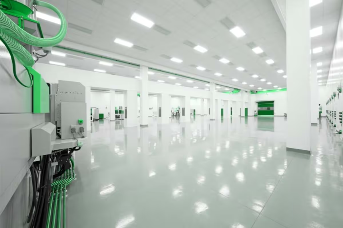
- Semiconductor construction is unusually demanding scope. Cleanroom construction to packaging-grade standards involves vibration-isolated structural systems, extensive process piping and specialty gas distribution, high-purity water systems, redundant electrical service, and mechanical systems with tolerances far beyond commercial work. The trade content per square foot is among the highest in the industry.
- The construction window is long and front-loaded. With cleanroom operations targeted for Q4 2028 from an August 2026 groundbreaking, there is roughly a 26-month construction program, and the process fit-out packages will run through 2028.
- Local labor markets will tighten measurably. A project of this scale in a metropolitan area the size of Greater Lafayette will absorb electricians, pipefitters, sheet metal workers and instrumentation technicians from a wide radius. Contractors on unrelated projects in central Indiana should expect wage pressure and reduced crew availability.
Implications for owners, developers, contractors and subcontractors
For owners in the Midwest, the labor absorption effect is a scheduling risk to price now. AGC and NCCER's 2026 workforce survey found that among firms reporting workforce effects from data center projects, 58 percent cited greater competition for skilled workers and 49 percent cited increased wage pressure, per Engineering News-Record. Semiconductor fabs produce a similar effect. Projects bidding in central Indiana between now and 2029 should assume less competition and higher labor cost.
For general contractors and specialty subs, the supplier ecosystem is where the accessible opportunity sits. More than 100 partners across materials, components and equipment implies supporting industrial facilities, warehousing, distribution and office space in the region, and that work is bid by regional firms rather than by national mission-critical specialists.
For firms in upstate New York, the parallel is direct. Micron's $12.0 billion Fab 1 Phase 1 in Clay, New York was among the largest projects to break ground nationally in July, per Dodge Construction Network. West Lafayette is a preview of what a semiconductor construction program does to a regional labor market, and Western New York contractors should be studying it for exactly that reason.
For workforce planners, the Purdue model is the transferable piece. Purdue launched the nation's first comprehensive semiconductor degrees program in 2022 and now has more than 800 undergraduate and graduate students pursuing semiconductor credentials or participating in the SCALE program, per Purdue. The talent pipeline was a stated factor in the siting decision.
What to watch next
- Contractor and design team announcements, which will indicate whether process and cleanroom scopes are going to national specialists or regional firms.
- Progress toward the Q4 2028 cleanroom milestone. Semiconductor schedules compress and slip frequently, and the Q3 2029 HBM4E production target depends on it.
- Whether SK hynix expands beyond packaging into front-end U.S. production. Kwak said the company aims to build an advanced memory supply chain in the United States and expects Indiana to be a key HBM base by 2030.
- Additional CHIPS-supported groundbreakings, which would signal whether the manufacturing construction decline is bottoming or continuing.
Bottom line
A more than $4 billion advanced packaging fab with a Q4 2028 cleanroom target, second-half 2029 mass production, roughly 1,000 permanent jobs, about 7,000 total direct and indirect jobs and $458 million in finalized CHIPS funding is a genuinely large industrial construction program starting at a moment when U.S. manufacturing construction spending is down 21.7 percent year over year. For contractors, the immediate read is a 26-month, process-heavy construction window in central Indiana and a corresponding tightening of the regional craft labor market. For everyone else, it is confirmation that AI-driven demand is the mechanism now sustaining large-scale industrial construction, in packaging and memory as much as in the data centers those chips will fill.
Sources
- Purdue University, "SK hynix breaks ground on $4 billion advanced packaging production facility in Purdue Research Park" — https://www.purdue.edu/newsroom/2026/Q3/sk-hynix-breaks-ground-on-4-billion-advanced-packaging-production-facility-in-purdue-research-park/
- State of Indiana, "Gov. Braun Breaks Ground on SK hynix Semiconductor Packaging Fab in Indiana" — https://events.in.gov/event/gov-braun-breaks-ground-onskhynixsemiconductor-packaging-fab-in-indiana
- Reuters, "SK Hynix to start AI chip output in Indiana in 2029, sees memory shortage through 2030" — https://www.reuters.com/world/asia-pacific/sk-hynix-holds-groundbreaking-ceremony-4-billion-indiana-ai-chip-packaging-2026-08-27/
- NIST CHIPS Program Office, SK hynix (Indiana) — https://www.nist.gov/chips/sk-hynix-indiana-west-lafayette
- Associated General Contractors of America, July 2026 construction spending analysis — https://www.agc.org/news/2026/09/01/construction-spending-declines-july-june-and-year-earlier-contractors-cope-soft-demand-most-types
- Dodge Construction Network, "Construction Starts Rebound 25.6% in July" — https://www.construction.com/construction-starts-rebound-july-2026/
- Engineering News-Record, "Even as Contractors Cut Headcount, 73% Still Plan to Hire" — https://www.enr.com/articles/63618-even-as-contractors-cut-headcount-73-still-plan-to-hire

Discuss an Upcoming Project


